BREAKING: Columbia University engineers have just unveiled a groundbreaking 160 nanometer metasurface that significantly enhances photon generation, paving the way for next-generation quantum chips. This revolutionary device, developed by a team led by Chiara Trovatello, promises to transform quantum hardware into more compact and efficient forms.
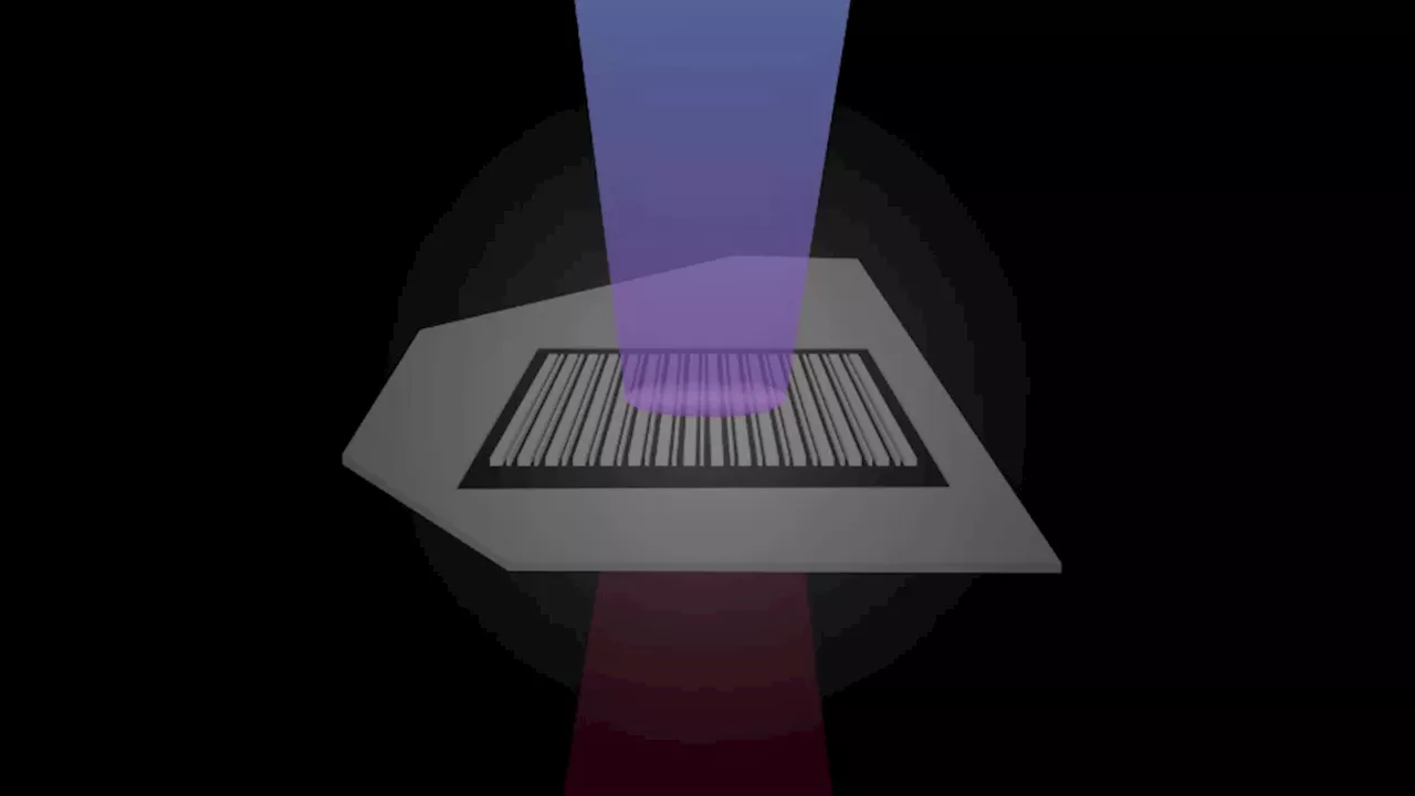
In a major leap for quantum technology, researchers at Columbia Engineering have successfully created an ultrathin metasurface capable of boosting nonlinear optical effects at the nanoscale. This innovative approach builds on previous work where a crystalline device of just 3.4 micrometers thick was able to generate entangled photon pairs. The new metasurface, however, slashes that scale down to a mere 160 nanometers.
The team utilized artificial patterns etched into ultrathin crystals to unlock new optical behaviors, a technique that Trovatello describes as a “successful recipe” for enhancing nonlinearity while maintaining sub-wavelength thickness. “Quantum hardware demands compact components,” she stated, underscoring the urgency of making qubit sources smaller and more manageable.
Previously, the group had achieved photon generation using periodic poling to align layers of molybdenum disulfide. The latest study, however, takes a different and more efficient route. PhD student Zhi Hao Peng carved nanoscale lines into a molybdenum disulfide flake, resulting in a remarkable 150-fold increase in second harmonic generation compared to unpatterned samples. This process allows two photons to merge into one with double the frequency, a significant breakthrough in photon generation technology.
“This design enhances nonlinear effects far beyond what traditional optical optimization can achieve,” Peng explained, emphasizing the transformative potential of this new approach. The implications are vast, as current qubit sources are often large and cumbersome, necessitating extensive equipment rooms. Trovatello’s team aims to shrink these sources, making quantum technologies more scalable and accessible.
Furthermore, the fabrication process has been simplified. Senior investigator Jim Schuck notes that while nonlinear crystals are crucial for many photonic technologies, they are often brittle and challenging to manufacture. Peng’s method, however, utilizes standard cleanroom tools, streamlining the production of these advanced materials.
The theoretical collaborators of the study helped identify optimal patterns for achieving strong nonlinear responses. Michele Cortufo highlighted the importance of alternating line widths for creating “nontrivial behavior” in such thin flakes. Andrea Alu emphasized that these engineered nonlocalities could lead to “compact, integrable platforms” for nonlinear optics.
The metasurface operates at telecom wavelengths, which facilitates easier future integration into existing technologies. Schuck envisions a future where this device could lead to fully on-chip quantum photonics, significantly advancing the field.
This groundbreaking research is published in the journal Nature Photonics, marking a pivotal moment in the quest for more efficient and compact quantum systems. As the team continues to refine their techniques, the future of quantum technology looks brighter than ever.
Stay tuned for further updates on this developing story, as Columbia engineers continue to push the boundaries of quantum innovation. This could very well be the key to unlocking the next generation of quantum computing and communication technologies.